The gainclone proves to be a great amp, however it does not have the power I needed – as it clips easily at moderate volumes on my speakers. I needed something as easy, but more powerful. This is when me and my friend Daniel found the datasheet of TDA7293. This IC can run up to 120V, low distortion, and can easily be paralleled.
Following our findings, we searched the internet to find more information for the TDA7293 schematics. We found several solutions, however we found out that the components are a little too much that point-to-point layout is not as easy as the gainclone, especially when there are so many connections and wirings.
We therefore searched the internet for PCBs for the TDA7293. We found a german site that sells a PCB that can place 2 TDA7293s (left and right channel), and have options for parallel. This is the only PCB that can be configure to parallel mode. However that also means that we need to order 3 boards if we wanted to parallel 3 TDA7293s (for 2 channels).
We then decided to do our own PCB. We decided on running 3 ICs in parallel as it is easier to layout the PCB compare to even more ICs. With 2 ICs, driving 4 ohm load is very limited for anything above 40V, and this would not provide enough drive for a real 4 ohm load. Besides, Linn Klimax Twin uses 3 TDA7293 as well.
I then get down to Protel to create the schematic and the PCB layout. Between each revision, Daniel will suggest this and suggest that, to improve the schematic and layout. On the 2nd revision, I etched a board and we tested with a few TDA7293 to make sure the schematic is working as planned. We celebrated when we heard music, but soon I’m back to my computer for the final few revisions to send for professional PCBs fabication.
That’s how the PI7293 – Parallel Inverting TDA7293 came about. The amp uses 3 TDA7293 per channel. By using a 35vac transformer to run at 49vdc, it can provide 100w into 8ohm, or 200w into 4ohm. It is also possible to provide an seperate inverted signal into another PI7293 to bridge 2 PI7293 amps.
Schematic
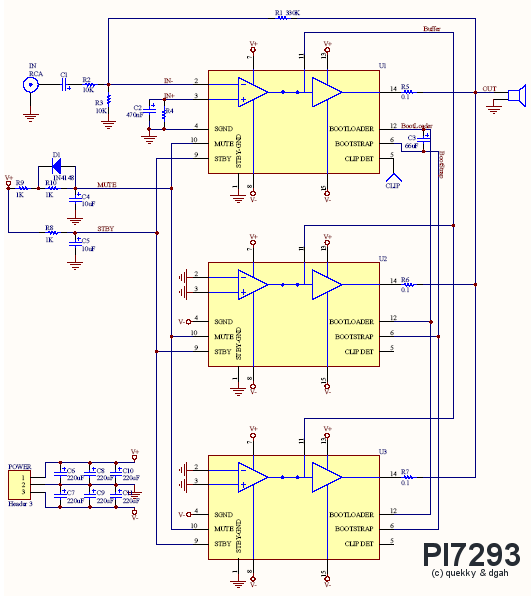
PI7293 uses an inverting configuration.
The gain is set by R1 and R2. R3 sets the noise gain. The recommended gain is 33. This is to make sure the amp remains stable without a connected input source, or when the input impedance is higher than around 2.7k ohms (as it might when connected to a volume control pot).
R4 is added to the V+ input to balance the resistance seen at both input ports. This is to make sure the output offset voltage remains low. An optional capacitor bypasses the R4 resistor at audio frequencies to establish a ground reference for the amplifier.
With the recommended values for R1 to R4, the measured output offset voltage for Daniel’s completed module is below the measurement limits of his multimeter! (<+/-0.5mV)
Capacitors C6 to C11 are power supply decoupling caps. The recommended values runs from anything above 47uf each to 1000uf or more. This assumes the usage of substantial power supply reservoir caps in the power supply itself though.
R8, R9, R10, D1, C4 and C5 forms the turn-on/off muting controls, are present to prevent turn-on and turn-off thumps. If desired, this could be controlled from a switch to provide user selectable mute and standby modes.
R5, R6 and R7 are optional ballast resistors to ensure current sharing in the 3 output devices. These could be first installed to ascertain current sharing, then removed later if so desired.
C1 is the input coupling cap and a BG-N cap is the preferred device here. The cap is optional though, and the resistor values specified are optimized without it in circuit.
All in all, there are just 25 components including the ICs for the fully rigged option. We use just 21, and you could get by with even less than that.
| Recommended values: | |
| Gain | 33 or more |
| R1 | 330k audio grade |
| R2 | 10k audio grade |
| R3 | 10k audio grade |
| R4 | 5.1k audio grade |
| R5,R6,R7 | 0 to 0.33ohm |
| R8,R9,R10 | 1k |
| C1 | BG N 4.7/50v |
| C2 | 220nF to 470nF |
| C3 | 66uF |
| C4,C5 | 10uF |
| C6 to C11 | 220uF to 1000uF |
PCB
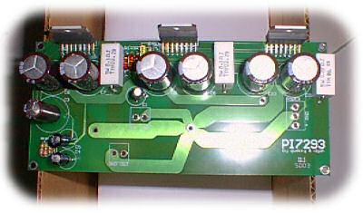
The layout of the PCB is well-spaced, with the important components as near to the 3 TDA7293 ICs as possible. Having a professional-done PCB means that we can use double-sided PCB, thus allowing us to use almost no jumpers yet have a short path for the signal. The input signal have a very short path to the master TDA7293 IC.
Even though it looks spacious, the size of the board is only 16.5×7.3cm.
The design highlight of the layout is in the very careful layout of the ground returns. Note in particular the very explicit “star” ground you see in the lower half of the board.
The construction of the amp is very straightforward; it can take less than 10 minutes to populate a board.
Power Supply
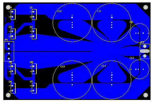
We use individual diodes as bridges, having 2 bridges for each channel. Any series of the MUR can be used, as long as the diode reverse voltage is above the voltage of the transformer output. We chooses MURs from onsemi due to their fast recovery time, and low voltage dropout. However you can use any other diode you like. Heatsinking the diodes is optional, as they do not get warm at all.
The PCB of the power supply allows us to use any size of caps after the bridges, up to 4 20000uF as long as they fit well on PCB. We can add another 2 smaller caps when needed.
This power supply board can also be use for other purpose if needed, e.g. other DIY amps or other preamps that I might build in the furture.
I etched the PCB at home using photosensitive boards. The size of the board is 15x10cm.
Update: Drawing Files
[Year 2018] I’ll not be able to provide the actual PCB anymore after over 10 years. I’ll provide the drawing files as-is for free, you can use the files to create your own PCB. Note these files are provided as-in and no support will be provided